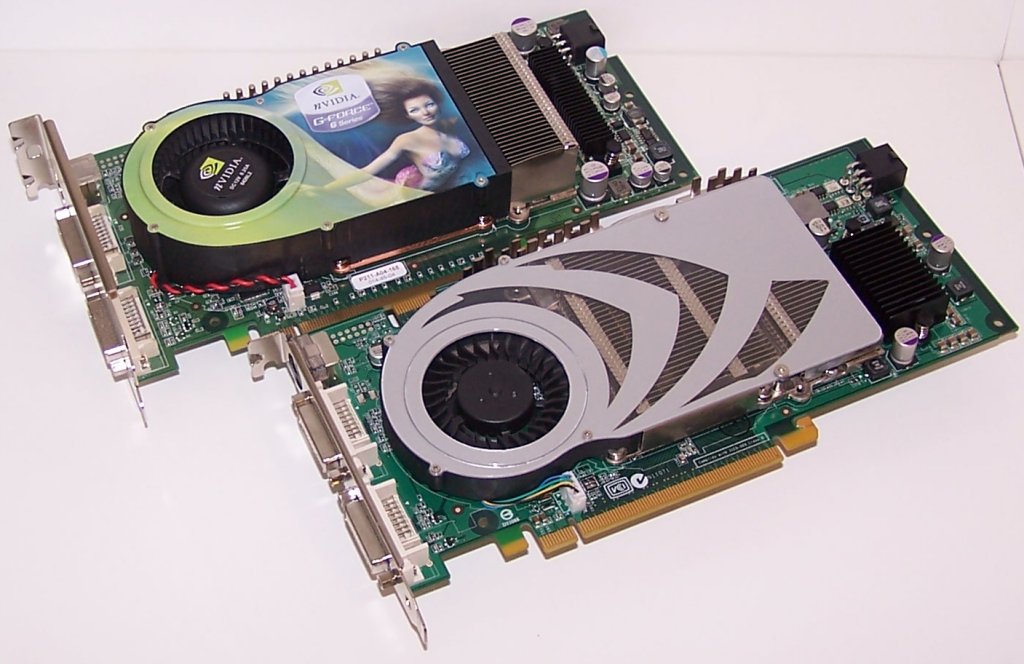
The BoardPresently the GeForce 7800 GTX is the only 7800 product announced and currently is said to be the highest performance product that NVIDIA will announce for this series of boards, at least right now. Here we'll take a closer look at the 7800 GTX board.
The clock speed increases for the GeForce 7800 GTX are fairly modest in relation to the previous high end 6800 Ultra, with a 30MHz core increase and a 50MHz memory clock speed increase. Despite the relatively low core clock speed increases, the wider fragment pipeline in conjunction with the shader changes should still provide a healthy increase, theoretically in excess of 2x in shader tests. We suspect that the reason for not using faster RAM may be down to availability of faster chips at this point in time.
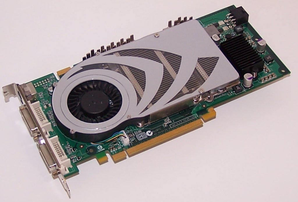
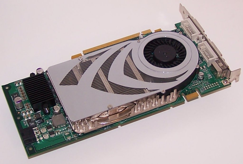
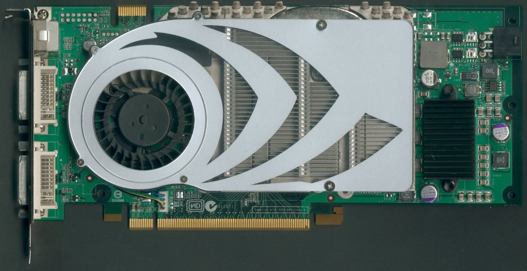
One of the most immediately obvious elements of the 7800 GTX board is the fact that NVIDIA have kept it down to a single slot design, with a fairly large, heatpiped, aluminium heatsink over the core with the fan pushing the air internally to the back of the board. The board itself is fairly long, standing at a PCB length of around 229mm, which is around 14mm longer than the 6800 Ultra. The PCI Express interface can provide a maximum of 75W and a single additional internal PCI Express power connector is required to power the boards - NVIDIA are keen to point out that they have made significant alterations to the power management of the G70 chip, including cycling down unused parts of the die, such that although there is increased performance the 7800 GTX actually has a lower power utilisation than the 6800 Ultra does. Update: G70 features an on-chip thermal diode that the 7800 GTX board can reference core temperature information from such that the fan speeds are scalable dependant on temperatures, allowing quiet operation in 2D / low utilisation scenarios with the fan scaling up to increase airflow in high utilisation situations.
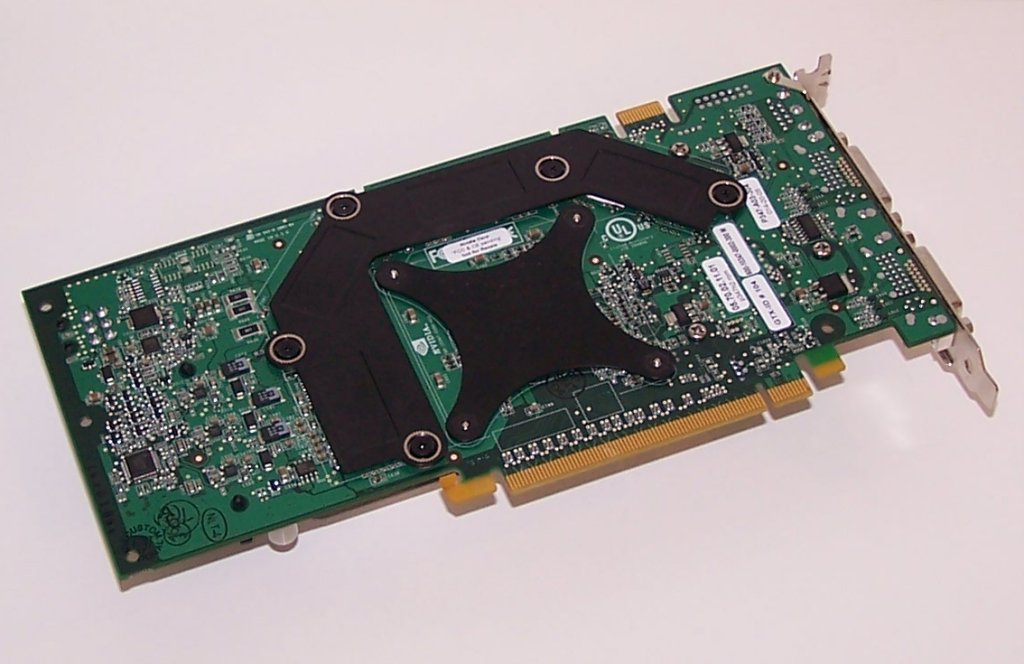
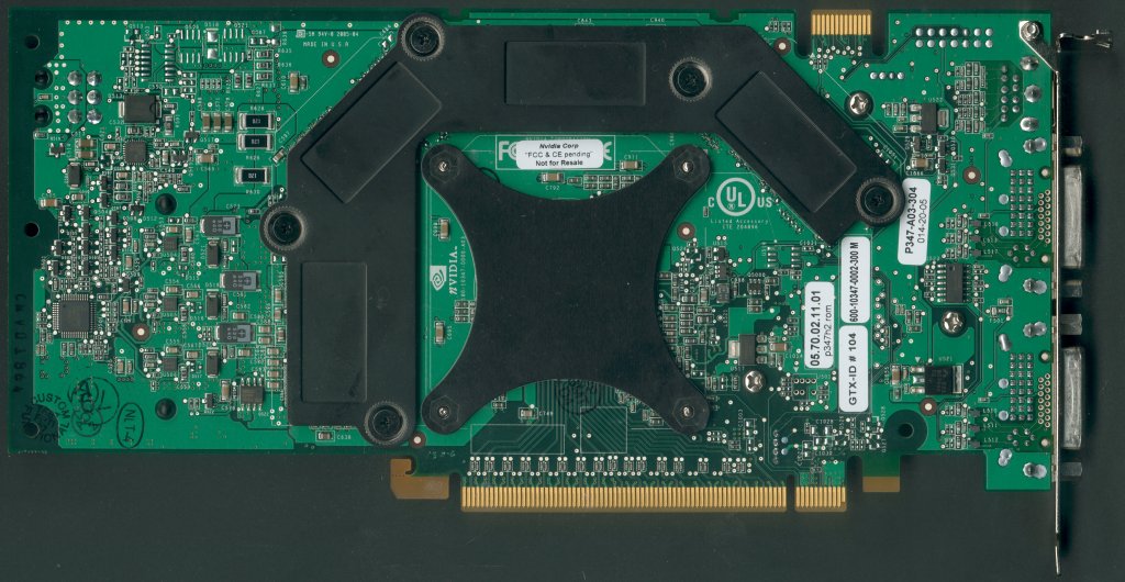
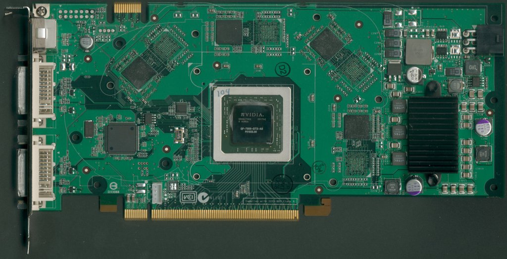
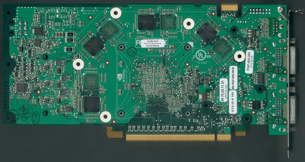
Removing the heatsink reveals exactly how large the die size of the 7800 GTX is and is primarily responsible for the board estimated retail price of $599. We can see that the board uses the same type of memory layout as featured on the NV40, however on this occasion the memory chips are distributed on the front and back, probably ready for population of the remaining free spots on the opposing sides of the currently populated places to get to 512MB configurations - we have already seen Samsung 512Mb 700MHz GDDR3 chips and these are slightly more rectangular in shape so perhaps the distribution of the modules is to more easily facilitate these types chips and get to 512MB with fewer, high density chips. The board features the same SLI connector as other SLI capable GeForce 6 Series boards so current connectors are still compatible. This reference board also features two DVI outputs. |
|||||||||||||||||||||||||||||||||||||||||
- NVIDIA Fermi GPU and Architecture Analysis
- ATI Cypress Gaming Performance Analysis
- ATI Cypress GPU and Architecture analysis
- ATI RV740 GPU and Architecture Analysis
- NVIDIA GT200 GPU and Architecture Analysis
- Dave Kirk - NVIDIA Tesla Launch
- Andy Keane Interview & Tesla Adoption/Deployment
- Travelling in Style: Beyond3D's C++ AMP contest - WINNER ANNOUNCED
- Was Harry Potter actually into rendering? Beyond3D's first ever book review
- E3 2011: Behind Closed Doors - Witcher 2 Xbox 360... and a Nurse
- Diving into Anti-Aliasing
- Q&A with Visceral's Technical Art Director Doug Brooks on Dead Space 2
- A speculative look on the Wii U GPU
- Ian Buck - NVIDIA Tesla Launch
- AMD's John Bridgman on Radeon, Linux and Open Source 3D
G70: NVIDIA GeForce 7800 GTX Review - Page 4
Published on 22nd Jun 2005, written by Dave Baumann for Consumer Graphics - Last updated: 20th Jul 2007
Page Navigation
Site width adjust
![]()
![]()
Reset width
Privacy Policy