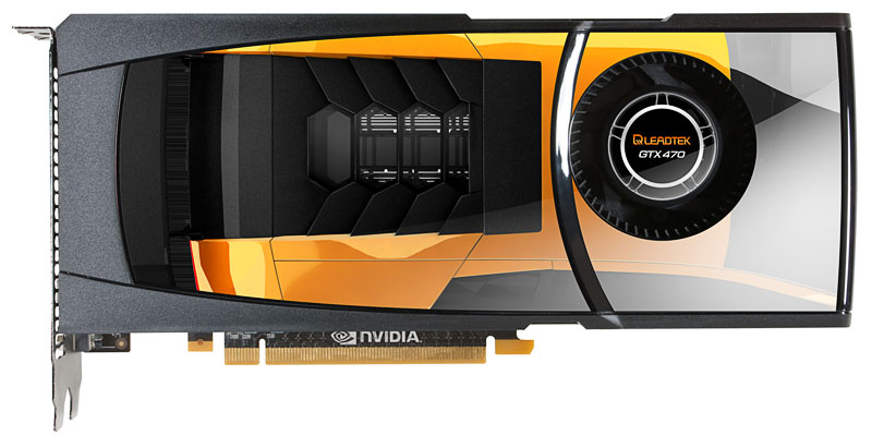
Leadtek Geforce GTX 470
The GeForce GTX 470 was one of the two initial Fermi incarnations, the other, as mentioned, being GTX 480. We didn't go for the kill and opted for buying the former, since we considered it more than adequate for our nefarious goals.
We went for the cheapest board we could find, which in our case ended up being the Leadtek version – still the base reference design, but with an odd sticker to rice it up. It's worth noting that in the period since Fermi's launch and your reading of this article, NVIDIA has managed to fill out more slots in its lineup, now having numerous products in the GTX 450-480 range of numerical IDs -- everything from 465 upwards is based on GF100, whereas the 460 and the recently launched 450 are based on specific derivative dies, GF104 and GF106 respectively.
On the left-hand side of the page you'll find a quick breakdown of the theoretical numbers the 470 boasts. If you go and look up the specs for the GTX285 posted by other more productive hacks, you'll probably note that some numbers go down, somewhat unexpectedly – we're looking at you, ALU clock, and you texture sampling rate, and you too pixel fillrate! Now, the official party line is that whilst unit counts were down-scaled (in the case of samplers), efficiency has gone up enough to compensate for that – and we're more than ready to confirm that for very specific cases. Outside of those, however, a GTX285 will be slightly more muscular than its newer sibling.
From the "oh wow, bump!" side of the fence we have a major increase in triangle setup/raster rate, albeit certain restrictions we'll detail apply there too (this is why we're quoting an interval, rather than a single fixed value), and you shouldn't really expect 4 triangle per clock to make a showing in practice. This is one of the significant novelties GF100 brings, and after spending time with it we think the new, distributed geometry engine is quite nice, if brittle in spots, and we do see this as being the evolutionary path to be followed on that front going forward.
Interfacing with memory is one of the areas that gave NVIDIA some pain as they were bringing out Fermi, and the move to GDDR5 wasn't their smoothest ever. This is quite apparent when considering that whilst the memory chips used on the 470 (1 ns chips from Samsung, that is) are rated at 1 GHz (4 GHz effective) they're run at a notably lower 837 MHz (3.348 GHz effective). Interfacing with them via a 320-bit bus means that the 470 gives you 133.9 GB/s of bandwidth to VRAM. Not too shabby, but also not as high as it could have been, or indeed that we were expecting it to be at some point in the pre-launch era.
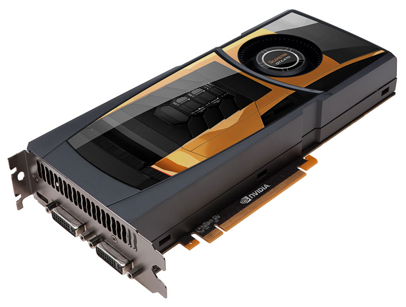
Not following in the footsteps of ATI's 5870 boards (those were looong), the GTX 470 board is roughly 24.1 cm long, making it somewhat more appealing to those with overly tight cases, or silly SATA port orientations. Cooling is achieved via a 2-slot, out-blowing, aluminium heatsink, copper heatpipe solution -- say that really really fast! You'll also need dual 6-pin power connectors to supplement the x16 PCIe slot when it comes to powering this shader of pixels. The noise this quasi-devilish yet common contraption generates is subjectively higher than the one put out by a 5870, both at idle and under load, and it can be a tad unnerving in the latter case, albeit not as much as other solutions from times gone by.
In terms of connectivity, NV decided to equip its creation with two dual-link DVI ports and a mini HDMI one. The HDMI output is compliant with revision 1.3a of the spec, so we could insert a laundry list of features that come with this compliancy, but being ultimately evil we won't do it and encourage you to embark on your own quest for that knowledge!
Cover the stuff you already knew and probably read about ten times before – done! So let's check out the rig we used, and also properly introduce the new Beyond3D Testing Suite!