A Red PCB With A Small Chip On Its Belly
Whilst you'd not typically expect GPUs intended to be the basis of sub 100$ SKUs to be all that interesting or novel, RV740 doesn't want to play nice with that rule. For all intents and purposes, it was the first 40nm GPU out. On top of that, instead of the usually castrated unit counts, its configuration is unexpectedly beefy, if one ignores the mainstream and pedestrian 128-bit memory bus.
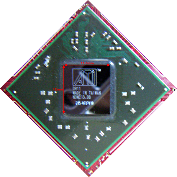
As you can see, TSMC's 40nm process allowed ATI to cram ~826M transistors into a petite, slightly asymmetric 12x11.5mm die (give or take). Doing a quick and semi-irrelevant -- albeit fun -- comparison, that equates to a transistor density of about 5.98M per square millimetre which compares favourably to the 3.67M per square millimetre one which characterised RV770 on TSMC's 55nm. Whether or not this is indicative of things to come is anybody's guess, at this point at least.
Peeking slightly under the hood (don't worry, we'll be ripping it of soon enough, this is just the tease before the please), we find staring back at us the tried and true RV770 recipe, which means a fully unified DX10.1 compliant architecture paired with quite a bit of SRAM and the mysterious, not-yet-used-soon-to-be-obsoleted tessellator, a hardware block with support that exists outside of current and future API specs (albeit it can be accessed and interfaced with fairly easily).
Memory interfacing is handled via an optimised crossbar (due to area and memory density, and a departure from the ring bus that dominated ATI memory interface designs since the X1800), that is connected to 512 MiB of GDDR5. Finally the whole enchilada interacts with the host via PCI Express 2.0 x16.
Have a nice picture of the creeper, before moving on to the next page: