NVIDIA GT200 Overview
The following diagram represents a high-level look at how GT200 is architected and what some of the functional units are capable of. It's a similar chip to G80, of that there's no doubt, but the silicon surgery undertaken by NVIDIA's architects to create it means we have quite a different beast when you take a look under the surface.
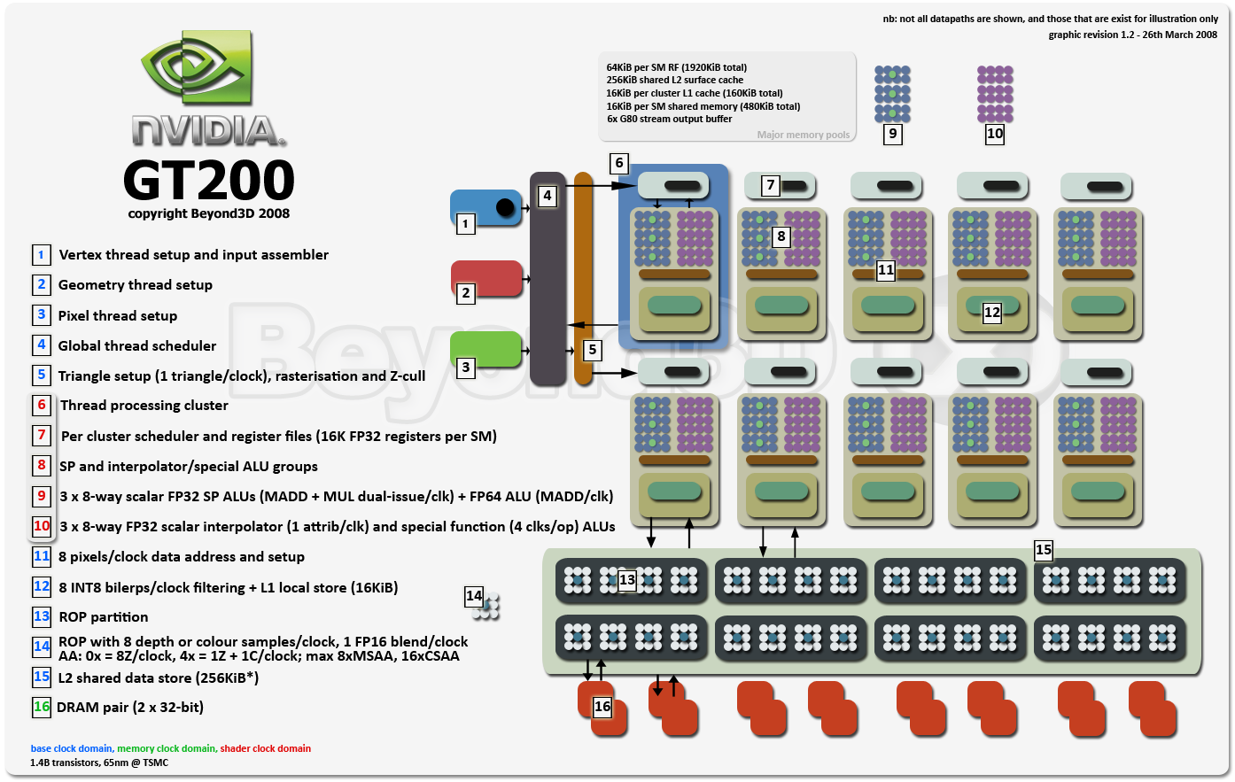
If it's not clear from the above diagram, like G80, GT200 is a fully-unified, heavily-threaded, self load-balancing (full time, agnostic of API) shading architecture. It has decoupled and threaded data processing, allowing the hardware to fully realise the goal of hiding sampler latency by scheduling sampler threads independently of, and asynchronously with, shading threads.
The design goals of the chip appear to be the improvement of D3D10 performance in general, especially at the Geometry Shader stage, with the end result presumably as close to doubling the performance of a similarly clocked G92 as possible. There's not 2x the raw performance available everywhere on the chip of course, but the increase in certain computation resources should see it achieve something like that in practice, depending on what's being rendered or computed.
Let's look closer at the chip architecture, then. The analysis was written with our original look at G80 in mind. The architecture we discussed there is the basis for what we'll talk about today, so have a good read of that to refresh your memory, and/or ask in the forums if anything doesn't make sense. The original piece is a little outdated in places, as we've discovered more about the chip as time goes by over the last year and a half, so just ask about or let us know about something that doesn't quite fit.