Command Processor
The first thing we see on the pipeline diagram mentioned before is the ‘Command Processor’. This is presently a unique feature for PC 3D graphics as this enabled P10 to be the first Multithreaded 3D device for the PC.
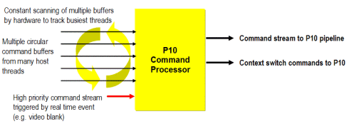
A normal 3D processor tends to be very wasteful when switching from one 3D task to another as the pipeline runs out of tasks to do and then has to request a new task from the CPU, with switching between different 3D applications becoming therefore somewhat stuttered. The command processor of P10 will actively and independently scan the various buffers from the CPU to keep track of where the work is and efficiently switch between one task and another – essentially a virtual VPU is setup per thread. Only one thread will have control over the entire pipeline at any one time, so two threads will not be able to share the resources of the chip and run simultaneously; however, the chip is able to completely context switch, meaning that the entirety of the current process can be dumped to memory and a new process uploaded in 15 micro-seconds, which is very quick by today's standards.
Now, this may not seem completely necessary in a gaming environment since how often are we going to be running more than one game or 3D app? Not very often. You could potentially see this having immediate benefits to 3Dlabs normal workstation market or even developers who need to switch between code and a 3D app often; however, this will become more important once the next generation Windows OS, codenamed Longhorn, becomes available. Longhorn uses a windows GUI system whereby each open window is actually drawn as a separate 3D application; in such an environment, the ability to switch from one thread (window) to another very fast will be very important.
The command processor also has another interrupt layer that can be used for efficiently switching between video applications.
‘Vertex Processor’
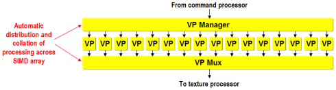
In the case of previous standard 3D chips, the vertex processing is hardwired specifically for its limited tasks, which means that nothing outside of those tasks can be achieved. However, the Vertex Processor in the P10 pipeline differs quite significantly from other Vertex Processor implementations as that it consists of a SIMD array of 16 32-bit floating point scalar processors, which are each capable of working on a separate vertex simultaneously.
The scalar nature of the processors means that the vertex processing can be done more efficiently than in conventional 3D graphics cards. For instance, GeForce uses Vec4 processing which is based on the principal that many of the operations being carried out are of 4 element vector ops (i.e. R:G:B:A or x,y,z,w) and a Vec4 unit is tuned to doing these operations very quickly. A Vec4 unit takes 4 processors per clock cycle to process a single instruction, regardless of the number of operations the instruction actually has, so when it has to process the less common instructions with 3 or 2 or 1 elements then it still has to use the 4 processors – thus wasting processing ability. In contrast, a scalar unit only uses the number of cycles that are actually in that instruction, which should therefore make such operations more efficient. GeForce4 Ti has 8 processing units,which equates to two Vec4 operations per cycle, whereas P10 houses 16 scalar units which equates to 4 Vec4 operations per cycle. Thus in raw processing terms, P10 has twice the raw vertex processing ability (or the same as Matrox's Parhelia); however, the more non-Vec4 operations are used the more efficiencies will be gained – 3Dlabs have suggested that up to 30% of instructions even in a standard OpenGL Transformation pipeline may not be Vec4 instructions. Another reason for utilising Scalar units is that these are compiler friendly – it's difficult for compilers to generate effective Vec4 code since it's good at some operations and not others. 3Dlabs also feel there will be no issues with latency by utilising Scalar units over Vec4 units either.
Unlike a basic FMAC (floating point multiply and accumulate) unit, each processor in the array is basically a mini-DSP core, with a 32-bit RISC-like instruction set, mathematical functions (Move, Add, Mul, MAdd, Min, Max, IntFloat, Fract, Trunc, Dot, Div, RSqrt, Log, Clipping), registers and register counters, temporary storage, and program storage – basically, this is a programmable device. The flow control of the processor array also includes conditional jumps, subroutines and loops, which is a superset of DirectX9 vertex flow control. The processor array isn't programmable by hand, but at the assembler level, which in this case is reasonably typical of any DSP assembler.
The maximum number of instructions that the vertex processor can handle at a time is 256 instructions (per unit); but, as mentioned before, the processors can use loops and subroutines so it can be much more efficient in the use of the 256 instructions. Ultimately the compiler will be able to multi-pass, so you can download one program and context switch it into a second pass if you wanted. The prototype OpenGL2.0 doesn't do this yet, but it should by the time OpenGL2.0 is ratified by the ARB. The goal is to take a 3MB Renderman shader (similar to the size used for 'Toy Story') and have it complied and running on P10 hardware – this hasn't been achieved just yet, but they hope to soon. Additionally the processors have 256 constant registers, 64 working registers and 22 opcodes.
Because looping operations are facilitated through programmability this allows the vertex processing array to do many things that hardwired units are usually created for and allows it to go beyond current hardwired methods; for instance the programmability allows it to handle as many as 200 lights in hardware. Multi-pass operations are achievable because the vertex processing array has access to memory, which means intermediate results can be stored, so any operation that is too large to fit in the caches can still be processed because they have access to main memory, which means that operations such as various forms of Higher Order Processing can be achieved. The vertex processor accesses memory by way of a GPIO program, which feeds it input data, and a context unit to write its results back to memory.
Some recent chips have had little hardware tessellation capability to allow HOS methods to be enabled; however, they are hardwired to perform a particular method of HOS (i.e. N-Patches, RT-Patches) and haven't been flexible enough to perform other methods. With the P10, its programmability allows any form of HOS that can be represented by a mathematical model to be achievable in hardware -- NURBS, N-Patches, surface subdivision, vertex blending, static and dynamic displacement mapping are all possible. It's difficult to gauge the relative performance P10's programmed HOS against current solutions at the moment since most HOS tessellation units available so far have been specific units that sit in front of the vertex processors and may actually be a bottleneck.
From a compiler point of view the parallelism is completely automatic; however, inter-processor communication does not occur so to optimise performance, operations need to be fashioned in such a way that multiple elements can be running in parallel on each of the processors – this can sometimes create interesting problems that require cunning solutions. An example of such an issue that has been resolved is Higher Order Processing. Normally each processor will process a single vertex; however, when calculating HOS the processor isn't looking at a single vertex point but a surface – hence it needs hence it needs to know about its neighbouring vertices. On the P10 such an issue would not fit naturally as there is no communication between processors. The method 3Dlabsdevised to circumvent this is by utilizing Barycentric coordinates so that the processing that needs to be done on the surface easily divides down into independent processing sets, as each point in Barycentric space can be processed independently from its neighbour.