Foreword
In our "R580: ATI Radeon X1900 XTX and Crossfire" article we took a look at the architecture of this new ATI chip and the performance it brings with its interesting configuration. With R580 scaling up the number of pixel shader processors fairly drastically, and yet not similarly scaling either the number of texture inputs or ROP outputs, some may still have the impression that R580 is a fairly imbalanced part.
In an effort to dig further into ATI's thinking behind the design of R580 and gain a greater understanding of the decisions that have lead to this process we decided to put some questions to them. In replay we have answers from Eric Demers, from ATI's Desktop Graphics Engineering group, as well as a few comments from Richard Huddy, who brings in the perspective from their ISV relations group, which has a front line role to play with developers and who plays an important part in shaping future hardware.
Introduction
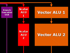
Ignoring the texture address processing and branching instruction capabilities the current "ATI ALU" (in R300-R5xx terms) consists of a Vec3/Scalar ADD ALU and a Vec3/Scalar MADD/ADD/MUL ALU, giving a peak instruction throughput of 4 instructions per cycle. Presumably this peak is the exception rather than the norm - have you profiled current applications to assess what type of average instruction throughput you are achieving?
[Eric Demers] I'd have to check with the compiler team, but on average, I think we see about 2.3 scalars per instructions being close to the average. Being able to do 2 full scalars (one using VEC and one Scalar) pretty much means that we are pegged out; as well the smaller ALU gets used a lot as well, giving an effective 2~4 scalars per cycle. As well, the average shader instruction (multiple scalars) to texture ratio is around 3 right now, and from what ISVs are telling us, it's likely to increase in the next few years. Consequently, the number of ALUs seems to be hitting the "sweet" spot for new applications (while being slightly underutilized for older apps) as well.
Can you give any background on what lead you to this a MADD and ADD ALU structure in the first place?
[Eric Demers] Well, initially, we wanted a prep stage that would allow all DX7 & DX8 fixed function operations (now shader operations) to execute in a single pipelined cycle in our HW. But then, we generalized the structure to give a full adder, do all DX9 input modifiers and also allow for some funkier functions, such as dual stage single cycle non-dependant LERP operations (which required the substract). It's ended up being a very good addition to the MAD stage, and the shader compiler does a great job of finding work for these units. We were able to save significant area by removing the multipliers from the pre stage. Even after these years of shader optimizations, we keep on finding new ways to use this shader core and get even more out of it. It ended up being a very good thing.
With R580 and RV530 this same structure still applies but with three times the number of Shader ALU's (although a texture address processor is shared between three ALU groups) - this means that the optimal instruction to texture ratio for these parts isn't just 3:1, but 3x2.3:1?
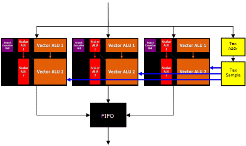
[Eric Demers] Yes, anything above 3:1 will max out the ALUs, giving the best overall performance. I would not multiply the 3 by the number of scalar ops per cycle, since the source operations for a texture address is most often vector. BTW, we don't do parallel shader execution; we execute parallel pixels on the same instruction in triplicate. But at the end, the aim is to keep all are units busy, all the time.