Processor
The processing block is at the heart of the Vertex Shader, this block executes the actual arithmetic instructions. As indicated before there are quite basic and simple instructions like ADD, there are a bit more complex instructions like DOT3 (Dot Product), and then there are really complicated instructions like a RSQ (Reciprocal Square Root). Now you might think: “it’s a chip it must be able to execute all that with little or no trouble, after all its maths and computers are really fast at thoseâ€. Reality is that maths for computers are pretty similar as maths for humans, simple things go very fast but complex things take a longer time. Adding 2 numbers is quite fast and easy for a human, calculating the reciprocal square root on the other hand might take quite some time. For a computer this translates to clock cycles, an addition might take 1 cycle but a RSQ will probably take quite some more time and silicon space to compute.
Lets look at a first example: “ADD R0, R1, R2â€. This instruction requires 2 source arguments to be summed and the result written out to a register. Remember that every register is 4 dimensional, so we can write this as follows:
| R0.x = R1.x + R2.x R0.y = R1.y + R2.y R0.z = R1.z + R2.z R0.w = R1.w + R2.w |
Every element is a full 32 bits IEEE Floating Point Value, so we have 4 floating point maths operations, being 4 additions. If the instruction was a “MUL†we’d have been looking at 4 floating point multiplications. What we have here is 4 “identical†maths operations (ADD, MUL, etc) but working on “different†data. The computer world has come up with an efficient structure to handle such problems, and this structure is known as SIMD: Single Instruction Multiple Data. Our addition/multiplication/etc is the single instruction and this operation gets executed on 4 different sets of data. In essence SIMD is nothing more than parallel processing.
Now the ADD and MUL both look very similar, 2 inputs and 1 single arithmetic operation being the addition or multiplication. So the structure needed to execute this is pretty simple and has only one stage. Let’s now look at something more complicated: “DP3 R0, R1, R2â€. This instruction executes a Dot Product of 2 vectors. The Dot Product of 2 vectors is defined as follows:
| R0.xyzw = R1.x * R2.x + R1.y * R2.y + R1.z * R2.z + R1.w * R2.w |
As you can see in this formula there are 2 vector inputs, but the output is a single scalar value that is written to all 4 components of the destination registers. Another big difference with the previous instructions is that we now have 2 arithmetic operations occurring at the same time: multiplications “and†additions. Even worse these mathematical operations are “dependent†on each other; you can not perform the addition until you have the result of the multiplications. This command actually has 3 stages: multiplication, addition and another addition. Basically what you end up with is a tree like structure at the top you have 4 multiplications, the results are fed into 2 adders and the result of those is fed into another adder. In a diagram this looks as follows:
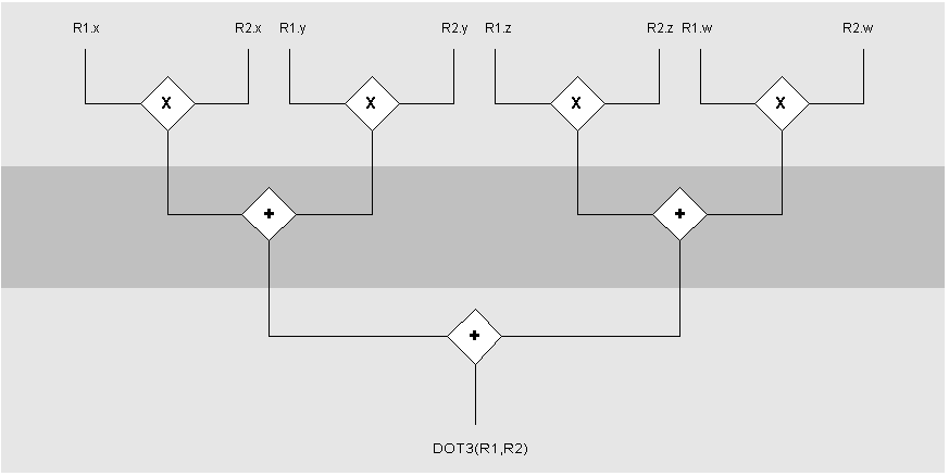
Notice the 3 stages indicated by grey bars
The difference in complexity between the simple ADD/MUL instructions and the more complex DOT3 instruction can again result in different hardware solutions. One option is to use a “single stage†and re-use that single stage multiple times to execute the more complex operations, another option is to directly support the complex operation which obviously results in more complex hardware and thus more silicon space being requirements.
Now with the second option we can either opt for a pipeline structure, where the first pipeline block does the four multiplications, the second block does two additions, and the final and third block does a single addition; or we can go for a single complex block. You might wonder what the difference is between 1 complex block and 3 simple pipelined blocks. The first case executes the operation in 1 clock, the second case can also execute one operation per clock, but the time between starting and ending the operation is actually 3 clocks (each pipeline block takes a clock) – so there is a delay of 3 clocks between starting the work and getting the result, this is called “latency†there is thus a latency of “3†for the second case while the latency of the first case is “1â€.
So which one is better? Now remember I started of by telling you that maths for a chip is not all that different than maths for a human. Doing something simple is easy and fast, doing something more complex takes more time… time translates to clocks cycles. The first complex block case has a lot of work to do within the time of 1 clock cycle, the second example has 3 clocks to execute the complex operation. This leads to the logical conclusion that the clock cycle time for the first example is going to be “longer†than for the second example. Pipelining allows clock speed to increase since you do lots of stages, but each stage is simple. Without pipelining you end up with complex operations that take a long time to come up with a result and hence long clock cycle times. This explains why the design of a chip immediately has an impact on the clock speed that can be achieved. A design with a single complex stage Vertex Shader will have a much lower clock speed limit than a pipelined design with lots of simple stages. Generally the longer the pipeline (more stages) the less complex the operation per stage and thus the higher the possible clock speed. The different Intel Pentium generations are allowing higher clock speeds because the pipelines are getting longer and longer. For a graphics chip pipelines lengths are limited and hence clock speeds are not quite as high since some operations for example can not easily be split into multiple pipelines stages. So in summary the arithmetic block at the hearth of our Vertex Shader can be designed in many ways: simple single stage that gets re-used through loop-back, single complex stage with a reduced clock speed, pipelined simple stages of different lengths. So again we have to conclude that there are different approaches possible, there is no single Vertex Shader definition.
Now I mentioned latency, latency is the dark side of pipelining as will become clear in the next section of this article.