VLIW core
The core of Crusoe is a VLIW architecture (Very Long Instruction Word). This is sometimes termed a post RISC (Reduced Instruction Set Computer) architecture as it fetches bundles of RISC instructions in 128bit (4 instructions) or 64 bit chunks (2 instructions) and then processes them in parallel according to ILP rules (Instruction Level Parallelism).
The bundle of instructions can look like this:
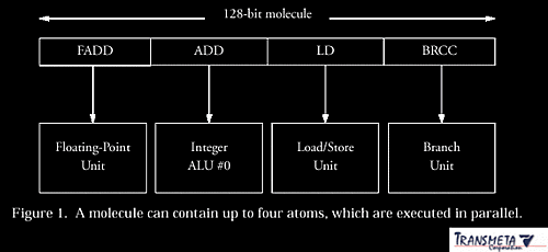
Crusoe is a four instruction wide VLIW architecture capable of four operations per clock cycle. The execution engine consists of:
- 1 Branch predict unit
- 1 Load Store unit
- 2 ALU's
- 1 FPU (Floating Point Unit)
Crusoe's core contains 64 integer registers for general-purpose use. These are used in the register renaming process that Crusoe has to use to maintain compatibility with x86.
A full discussion of VLIW architecture could take a whole paper - so see the references for more information (especially The PDF file titled - Technology behind the Crusoe processor on the Transmeta website).
Cache and memory
|
TM3200
|
TM5400
|
TM5600
|
|
| L1 Data cache size (KB) |
32
|
64
|
64
|
| L1 Instruction cache size (KB) |
64
|
64
|
64
|
| L2 Cache size (KB) |
0
|
256
|
256
|
| L1 D/I cache associativity |
8 way set
|
8 way set
|
8 way set
|
| L2 associativity |
N/A
|
4 way set
|
4 way set
|
The L1 cache on the Crusoe is quite large (96KB-128KB) as Transmeta are obviously trying to keep a high hit ratio. However as the cache size has to be quadrupled to double the hit ratio then large caches are generally considered to be inefficient with respect to LOAD/USE instruction/data latency.
The size of the L2 is fairly conventional, being identical to that of the PIII Coppermine series.
The TM5400 & TM5600 can be interfaced to DDR SDRAM main memory. This is quite a high performance interface with bandwidths of up to 2.1GB/s. There is not much of a need for this in PDA's!
Power consumption and design rules
Power consumption on the Transmeta processors is generally about ½ that of its x86 competitors, however continual manufacturing improvements are needed to keep competitive.
Power consumption in a processor is given using the following equation:
P=CV²f C = Capacitance, V = Core voltage f = frequency
By decreasing the design rules (the width of the gate or transistor interconnect wires), the transistors are made smaller resulting in less capacitance on the PN junctions and therefore lower power consumption.
The TM3200 was initially manufactured using 0.22u (0.22 micron) design rules. The TM5600 is the next version of the TM5400 and both are manufactured using 0.18u design rules that further reduce power.
Transmeta will move all production of the Crusoe to 0.13u design rules by Q4 2000 in combination with copper interconnect which drops chip power consumption (by reducing trace resistance) and increases performance through lower gate interconnect delays.